Transmission Electron Microscopy vs. Scanning Electron Microscopy
Electron microscopy is a key imaging technique in scientific research, allowing for the visualization of samples at extremely high resolutions. Two of the most commonly used types are Scanning Electron Microscope (SEM) and Transmission Electron Microscope (TEM). Both SEM and TEM rely on electron beams for imaging but differ fundamentally in their working principles, applications, and the kind of information they provide. Here we compare SEM and TEM in detail, focusing on their working principles, similarities, differences, the choice between them for imaging, and the types of specimens to which they are applied.
Principles of TEM and SEM
The SEM works by scanning a focused beam of electrons across the surface of a sample. When the electrons strike the surface, they interact with atoms in the sample, causing the emission of secondary electrons, backscattered electrons, and X-rays. The secondary electrons provide detailed topographical information, while the backscattered electrons provide compositional contrast. SEM detectors capture these signals to produce an image that shows the surface morphology and texture of the sample. The resolution of the SEM is typically 1-10 nm, depending on the instrument. In the SEM, the electron beam is raster-scanned across the sample, which remains stationary during imaging. The signals are collected pixel by pixel to form an image on a computer screen. The surface is illuminated by the interaction of the electrons with the sample, and this process results in three-dimensional images of the surface.
The TEM works by passing a beam of electrons through an ultrathin sample. The electron beam is accelerated by high voltages (typically between 80 kV and 300 kV) and passes through electromagnetic lenses to focus it on the sample. As the electrons pass through, they are scattered or absorbed to varying degrees depending on the density and composition of the material. The transmitted electrons are then focused by a series of lenses to form an image on a screen or detector. Unlike the SEM, which only images the surface, the TEM provides detailed information about the internal structure of the sample. TEM achieves a much higher resolution, often less than 1 nm, allowing it to resolve atomic arrangements and internal structures in biological and materials science samples.
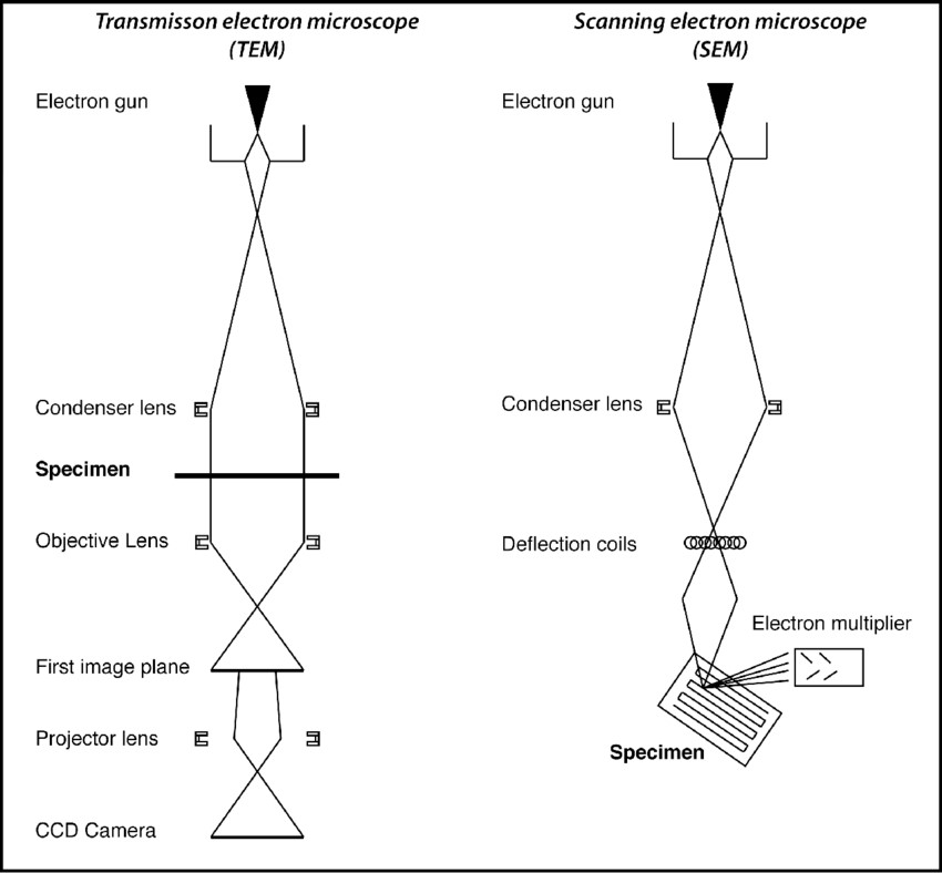 Figure 1. Schematic operation principles of a transmission- and a scanning electron microscope (Hagendorfer, 2011).
Similarities Between SEM and TEM
Electron Beams: Both SEM and TEM use electrons rather than light as the imaging source. Since electron wavelengths are much shorter than those of visible light, both techniques achieve much higher resolutions than optical microscopy.
Electromagnetic Lenses: Both SEM and TEM use electromagnetic lenses to focus the electron beam. These lenses control the magnification and resolution of the final image.
Vacuum Environment: Both techniques require a high-vacuum environment. Electrons can easily scatter when they interact with air molecules, so both SEM and TEM chambers are evacuated to prevent interference with the electron beam.
Image Formation: Both types of microscopes generate images based on electron-sample interactions. The differences in contrast and resolution depend on the way the electrons interact with the sample, but both techniques ultimately provide detailed images of the sample.
Differences Between SEM and TEM
Key differences between SEM and TEM are summarized in the table below:
Table 1. Differences between SEM and TEM.
| Scanning Electron Microscope (SEM) | Transmission Electron Microscope (TEM) | |
| Imaging Mode | SEM scans the surface of the sample and detects secondary and backscattered electrons that provide information about the surface morphology. | TEM transmits electrons through a thin specimen to capture internal structures. |
| Resolution | SEM typically achieves a resolution of 1–10 nm, making it excellent for surface imaging but less effective for internal structures. | TEM offers sub-nanometer resolution, making it ideal for studying the atomic structure and fine details of internal components. |
| Sample Thickness | SEM can handle bulkier and thicker samples because it only images the surface, and there's no requirement for electrons to penetrate through the specimen. | TEM requires ultra-thin specimens (usually less than 100 nm thick), as electrons need to pass through the sample to form an image. |
| Image Information | SEM provides three-dimensional-like images of surface morphology, which is useful for studying surface texture, topography, and the external structure of materials. | TEM provides two-dimensional images of internal structures at atomic resolution, which is ideal for studying cellular structures, molecular complexes, and crystallographic information. |
| Sample Preparation | SEM requires minimal sample preparation, mainly coating non-conductive samples with a thin metal layer (e.g., gold or platinum) to prevent charging. | TEM requires extensive sample preparation, including sectioning, staining, and embedding, especially for biological specimens. |
| Cost and Complexity | SEM is generally less expensive and easier to operate compared to TEM. SEM systems are more robust and require less maintenance. | TEM is more expensive and complex due to the higher resolution and intricate sample preparation. TEM also requires a more sophisticated vacuum and imaging system. |
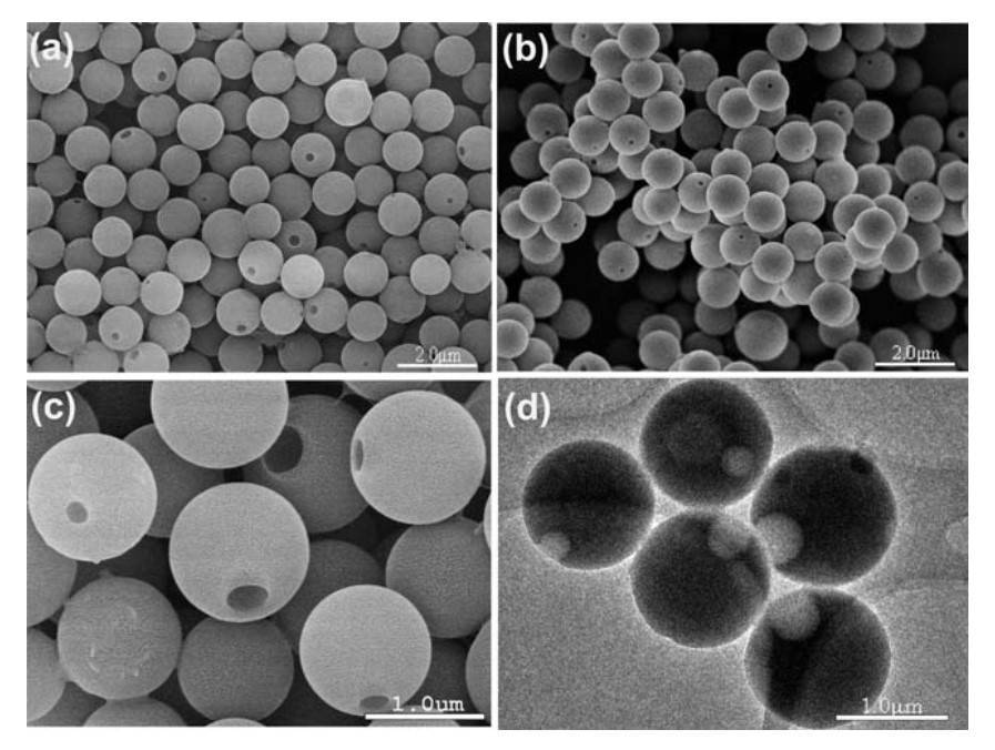 Figure 2. Studying the same sample with SEM and TEM. Typical SEM and TEM images of the monoporous polymer microspheres. (a and b) SEM images of spheres with different sized pores in their surfaces; (c) magnified SEM image of monoporous microspheres in (a); and (d) TEM image of microspheres in (a). Most of the microspheres have single hole, but not each one can be discerned, since many holes are hidden in the back of the microspheres (Zhu et al., 2011).
In conclusion, SEM and TEM are both indispensable tools in modern scientific research, offering different but complementary insights into the structure of materials and biological specimens. SEM's strength lies in its ability to image surface morphology and handle larger, thicker samples, making it ideal for surface analysis and industrial applications. TEM, with its atomic-level resolution and ability to image internal structures, is crucial for studying cellular structures, nanomaterials, and molecular assemblies. Understanding the working principles, similarities, and differences between SEM and TEM helps researchers choose the appropriate technique for their specific needs, whether it be surface characterization, internal structure visualization, or atomic-level resolution. The decision between SEM and TEM depends on the resolution required, the nature of the sample, and the type of information needed from the imaging process.
At Creative Biostructure, we offer comprehensive SEM and TEM services tailored to your research needs, delivering high-resolution images and detailed analyses. If you're unsure which technology best suits your project, our experienced experts are here to guide you in choosing the optimal approach. Contact us today to learn more about how our SEM and TEM services can support your research and accelerate your discoveries.
References
- Advanced transmission electron microscopy: Imaging and diffraction in nanoscience. Springer, 2017. Zuo, J. M.
- Ayache, J., Beaunier, L., Boumendil, J., Ehret, G., & Laub, D. (2010). The different observation modes in electron microscopy (Sem, tem, stem). In J. Ayache, L. Beaunier, J. Boumendil, G. Ehret, & D. Laub, Sample Preparation Handbook for Transmission Electron Microscopy (pp. 33–55). Springer New York.
- Hagendorfer, H. New analytical methods for size fractionated, quantitative, and element specific analysis of metallic engineered nanoparticles in aerosols and dispersions. Doctoral thesis, 2011.
- Zhu, M.-Q., Chen, G.-C., Li, Y.-M., Fan, J.-B., Zhu, M.-F., & Tang, Z. (2011). One-step template-free synthesis of monoporous polymer microspheres with uniform sizes via microwave-mediated dispersion polymerization. Nanoscale, 3(11), 4608.


