A Brief Introduction to Scanning Electron Microscope (SEM)
What Is the Scanning Electron Microscope?
A Scanning Electron Microscope (SEM) is an advanced imaging tool that uses focused beams of electrons instead of light to create detailed images of the surface of a sample. Unlike traditional optical microscopes, SEM can achieve much higher resolution, down to the nanometer scale, allowing for precise visualization of fine structures and surfaces. SEM is extensively used in material science, biology, chemistry, and industrial applications to analyze the topography, composition, and properties of various samples.
The SEM works by scanning a focused beam of electrons across the surface of the sample, causing secondary electrons to be emitted from the surface. These electrons are then collected by a detector to form an image. Because the wavelength of the electrons is much shorter than that of visible light, the SEM can capture images with much finer detail, which is often used to observe the morphology and composition of cells, tissues, and other small structures.
History of SEM
The origins of the SEM can be traced to the development of electron microscopy in the 1930s. The invention of the Transmission Electron Microscope (TEM) by Max Knoll and Ernst Ruska in 1931 marked the first use of electrons for imaging. However, the TEM required very thin samples and could only produce two-dimensional images.
The concept of a scanning electron microscope was introduced by German scientist Max Knoll in 1935, but the practical development of the SEM took longer. In 1942, Manfred von Ardenne, a German physicist, built the first working SEM prototype by improving on Knoll's idea. However, it wasn't until 1965 that the first commercially available SEM was produced by the Cambridge Instrument Company, led by Sir Charles Oatley and his student Vladimir Zworykin.
Subsequent advances in electron optics, vacuum systems, and detection methods have greatly improved SEM performance. Today's SEMs offer not only higher resolution, but also more sophisticated capabilities, such as energy dispersive X-ray (EDX) spectroscopy for elemental analysis.
Basic Principles and Instrumentation of SEM
The SEM operates based on the interaction between an electron beam and the sample surface. The basic components of a SEM include an electron gun, electromagnetic lenses, scanning coils, detectors, and a vacuum system. The principle of SEM imaging is grounded in the following steps:
Electron Beam Generation: An electron gun generates a focused electron beam by emitting electrons either through thermionic emission (using a heated filament such as tungsten) or field emission (using a sharp tip under high electric fields).
Focusing the Beam: The electron beam is focused to a fine spot using electromagnetic lenses. The size of the beam, which can be as small as a few nanometers in diameter, determines the resolution of the image.
Interaction with the Sample: When the electron beam hits the sample surface, it interacts with the atoms in the material, producing several types of signals, including secondary electrons, backscattered electrons, and X-rays.
Detection: These emitted signals are collected by detectors to form an image. The secondary electrons emitted from the surface layers of the sample provide high-resolution images with detailed surface information. Backscattered electrons emitted from deeper within the sample can provide information about the composition of the sample.
The resolution of the SEM depends on the size of the electron beam, and modern SEMs can achieve resolutions as fine as 1 nm, although this varies depending on the type of sample and operating conditions. In addition, SEMs offer a large depth of field, which allows for three-dimensional images of complex surfaces.
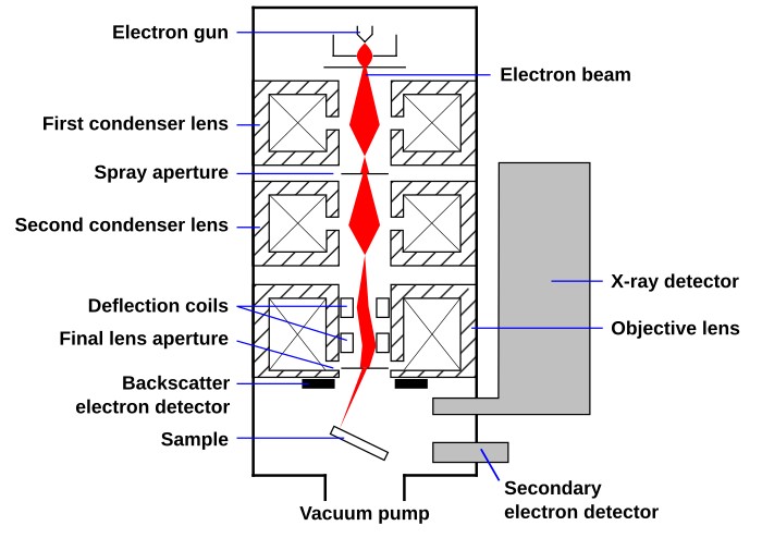 Figure 1. Schematic of a scanning electron microscopy.
Subdivision Techniques of SEM
Several advanced techniques have been developed to enhance the capabilities of the SEM for specific applications:
Environmental Scanning Electron Microscopy (ESEM): ESEM allows samples to be imaged in a low vacuum or even wet environment, which is particularly useful for biological and hydrated samples. This technique eliminates the need for conductive coatings and allows observation of samples in their natural state.
Focused Ion Beam SEM (FIB-SEM): FIB-SEM combines SEM with focused ion beams that can be used to mill, cut, or etch samples at the nanoscale. This is particularly useful for preparing thin sections for transmission electron microscopy (TEM) or for 3D imaging of material structures.
Cryo-SEM: In cryo-SEM, samples are frozen to preserve their native structure and then imaged in the frozen state. This technique is often used for biological samples that are sensitive to dehydration and high vacuum.
Energy-Dispersive X-ray Spectroscopy (EDX): EDX can be integrated with the SEM to provide elemental analysis. As the electron beam interacts with the sample, it excites the atoms, causing them to emit characteristic X-rays. These X-rays are detected and analyzed to determine the elemental composition of the sample.
Applications of SEM
In structural biology, SEM plays a critical role in imaging and analyzing the structure of cells, tissues, and macromolecular complexes. The high-resolution imaging capabilities of SEM provide valuable insights into cellular architecture and organelle arrangement. Some key applications of SEM in structural biology include:
Cell Surface Morphology: SEM is commonly used to study the surface morphology of cells and tissues. For example, SEM can be used to observe the microvilli on intestinal epithelial cells, the cilia on respiratory epithelial cells, or the intricate surface structures of cancer cells.
Virus and Bacteria Imaging: SEM has been instrumental in visualizing the morphology of viruses and bacteria. By providing detailed images of their surfaces, SEM helps to understand the mechanisms of infection and host-pathogen interactions.
Tissue Engineering: SEM is used in tissue engineering to analyze the scaffolds (membrane scaffold proteins) and matrices used to support cell growth. The technique helps researchers assess the topography and porosity of biomaterials, which are critical factors for successful tissue regeneration.
Biofilms: SEM is a valuable tool for studying biofilms, which are communities of microorganisms that form on surfaces. By imaging the structure and arrangement of cells within the biofilm, researchers can better understand biofilm formation and its implications in medical and industrial settings.
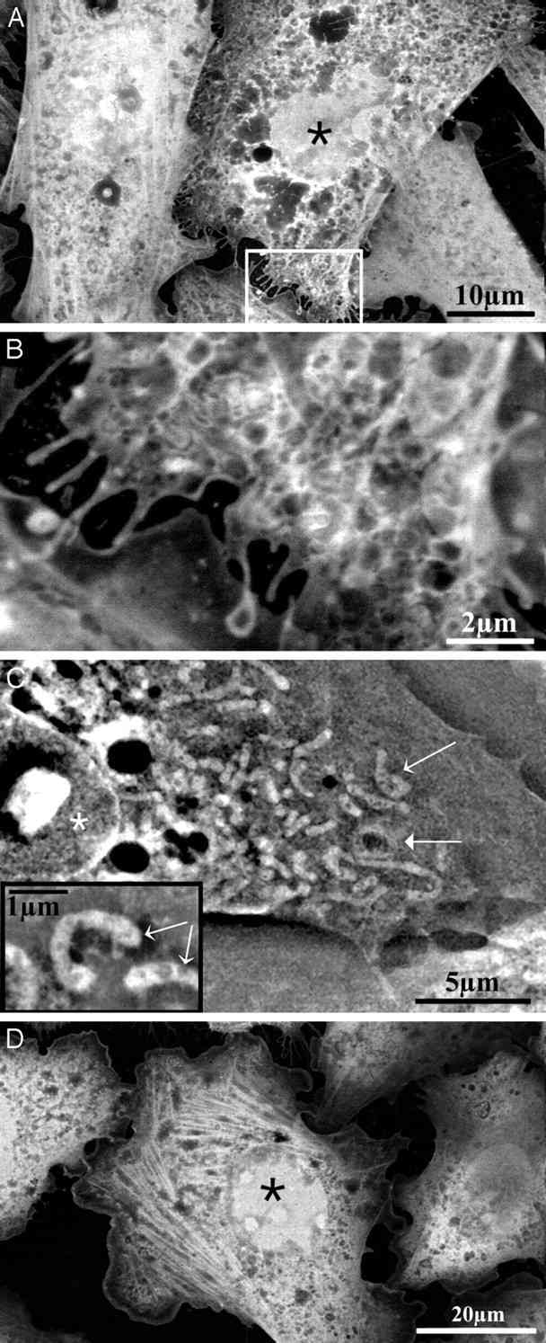 Figure 2. Imaging of stained cells with SEM. Asterisks denote nuclei, and thin arrows denote mitochondria. (A) HeLa cells grown on the membrane in normal growth medium, then fixed with paraformaldehyde, and stained with uranyl acetate (imaged at 12 kV). (B) Magnification of the marked rectangle shown in A. (C) CHO cell fixed with glutaraldehyde and paraformaldehyde, stained with uranyl acetate, and maintained in water (imaged at 30 kV). The thick arrow denotes a mitochondrion that surrounds a lipid droplet. (Inset) Higher magnification showing mitochondria (thin arrows). (D) Actin fibers in stained CHO cells. Treatment and imaging are as described for A (Thiberge et al., 2004).
In summary, the Scanning Electron Microscope (SEM) is a powerful imaging tool that provides unparalleled resolution and versatility for the analysis of a wide range of samples. With origins dating back to the mid-20th century, the SEM has become an essential tool in fields such as materials science, biology, and structural biology. Its ability to produce high-resolution images, coupled with advanced techniques such as ESEM, FIB-SEM, and cryo-SEM, allows detailed analysis of complex structures at the micro- and nanoscale. In structural biology, SEM has contributed significantly to our understanding of cellular structures, tissues, and microbial morphology, making it indispensable in modern scientific research.
At Creative Biostructure, we offer advanced Scanning Electron Microscope (SEM) services tailored specifically for structural biology research. Our high-resolution imaging capabilities provide detailed insights into the morphology and surface structures of biomolecules and materials. Whether you're studying biological specimens or complex molecular structures, our SEM expertise will support your research objectives. Contact us today to learn how our SEM services can help drive your discoveries and elevate your scientific endeavors. Let us partner with you in achieving breakthrough results in structural biology.
References
- Joy, D. C., & Pawley, J. B. (1992). High-resolution scanning electron microscopy. Ultramicroscopy, 47(1–3), 80–100.
- McMullan, D. (1995). Scanning electron microscopy 1928–1965. Scanning, 17(3), 175–185.
- Thiberge, S., Nechushtan, A., Sprinzak, D., Gileadi, O., Behar, V., Zik, O., Chowers, Y., Michaeli, S., Schlessinger, J., & Moses, E. (2004). Scanning electron microscopy of cells and tissues under fully hydrated conditions. Proceedings of the National Academy of Sciences, 101(10), 3346–3351.
- Zhou, W., Apkarian, R., Wang, Z. L., & Joy, D. (2006). Fundamentals of scanning electron microscopy (Sem). In W. Zhou & Z. L. Wang (Eds.), Scanning Microscopy for Nanotechnology (pp. 1–40). Springer New York.


