Application of Atomic Force Microscopy (AFM) in Physical Science
Atomic force microscopy (AFM) is a new surface analysis instrument based on physical principles and imaging through the interaction between scanning probes and sample surface atoms. It belongs to the third generation of microscopes after optical and electron microscopes. The invention of the atomic force microscope (AFM) provides a powerful tool for high-resolution detection of the physical properties of biological samples in the natural state at the micro-nano scale. It is a powerful supplement to traditional biochemical properties detection methods. In physics, AFM can be used to study the surface morphology, surface reconstruction, surface electronic state and dynamic process of metals and semiconductors, the surface structure of superconductors, and the charge density in electronic state layered materials, etc.
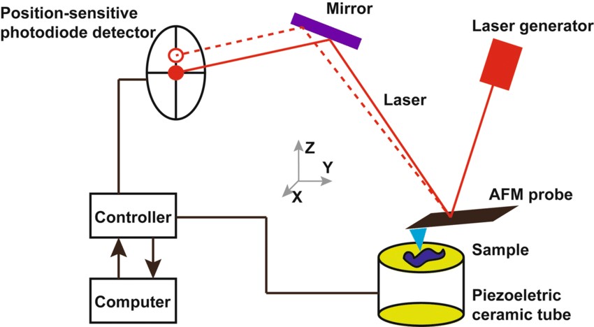
 Figure 1. Schematic diagram of AFM working principles.
Physical Science Applications of Our AFM Service
The application of AFM in physical science provided by Creative Biostructure mainly includes these aspects: surface topography, surface reconstruction, surface electronic states and dynamic processes, and charge density.
Surface topography
AFM has obtained atomic-resolution images of many different materials, including insulators and conductors. The atomic force microscope can not only realize the measurement of micro-force at the nanometer scale but also obtain information such as three-dimensional shape, fractal structure, lateral force, and phase boundary. Especially important, it can also realize the measurement of the process.
Surface reconstruction
The surface structure of metals can be deduced from the crystal structure, but metal surfaces are very complex. Diffraction analysis methods have shown that, in many cases, the surface forms a super crystalline structure (called surface reconstruction) that minimizes the surface free energy. With the help of AFM, the reconstructed images of some metals and semiconductors can be easily obtained.
Surface electronic states and dynamic processes
In conductive probe AFM, a sharp conductive tip is in contact with the sample. During this contact, a bias voltage is applied between the probe and the sample, and the current flow between the two is measured as the probe rasters across the surface, creating a conductivity or current map.
Creative Biostructure can offer you the different applications of AFM in physical science, giving you the information, you need to do great work. Please feel free to contact us for more information or a detailed quote.
Ordering Process
References
- Veerapandian M, Yun K. Study of atomic force microscopy in pharmaceutical and biopharmaceutical interactions-A mini review. Current Pharmaceutical Analysis. 2009, 5(3): 256-268.
- Hilmi I., et al. Research Update: Van-der-Waals epitaxy of layered chalcogenide Sb2Te3 thin films grown by pulsed laser deposition. APL Materials. 2017, 5(5).

